NanoSaintÉtienne
These technical systems are designed to support research. This is a team of 7 people which is open to industrial and academic partners.
The facilities are dedicated to 4 areas:
- Gratings elaboration
- Thin film deposition
- Processing substrates
- Profile analysis
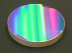
Gratings elaboration
Equipment :
Mask aligners : SET 702, Kloé UV-KUB-3
Interference lithography (grating period down to 300 nm)
Direct-write lithography : Kloé Dilase 750, DMO MicroWriter3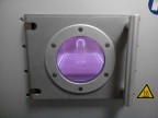
Processing substrates
Equipment :
Rapid Thermal Annealing (RTA) oven : Annealsys AS-One 100, up to 1250 °C
Ovens : up to 200-300 °C, operation under primary vacuum or humidity control
Oxygen plasma cleaner : Diener P100
Thin film deposition
Equipment :
Joule effect evaporation source : Al, Au, Cr, Pd
DC/RF Sputtering Systems : Al, Co, Cr, Cu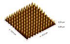
Profile analysis
Equipment :
Atomic force microscope : Bruker Dimension Icon, with options PeakForce QNM and Nano-DMA.
Profilometer : Bruker DektakXT
Optical microscope : Zeiss Axio Imager M1m
Spectrometry
Equipment :
Spectrophotometer : Agilent Cary 7000
Raman spectrometers : Jobin Yvon ARAMIS, Renishaw Qontor