Functional materials and surfaces
Credits : Sonia Barcet
The work of the group is centered on the structuring of materials at the subwavelength scale and their interaction with electromagnetic waves to realize optical or high-frequency devices. Multi-functional and multi-material approaches are used to address various applications: polarization control of laser sources, data marking for identity security, photocatalytic devices for indoor treatment, solar absorbers, sensors, isolators, imaging or nondestructive control, efficient energy converter.
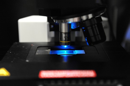
Such developments are based on the design and the electromagnetic modelling of the interaction between waves and micro-nano-structures. Realizations classically employ common planar photolithography and associated techniques.
Group expertise
Self-organization and controlled growth of metallic nanoparticles in mesostructured thin films. Plasmonic related effects.
Modeling of the electromagnetic behavior of nano-patterned structures, metallic NP arrangements, passive radio/micro-wave devices, photonic and HF jets
Interferential lithography at large scale (4’’) with short periods (200 nm).
Integrated devices based on magnetic materials for inductive or non-reciprocal functions.